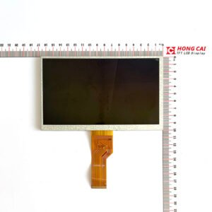
Description
NJ080IA-10D is an Innolux 8 inch LCD with 1024×600 resolution, TFT LCD module, 1500 cd/m² LED backlight, 40PIN LVDS interface.
| No. | Item | Specification | Remark |
| 1 | LCD size | 8.0 inch(Diagonal) | |
| 2 | Brightness | 1500 cd/m² | |
| 3 | Resolution | 1024 × 3(RGB) × 600 | |
| 4 | Display mode | Normally Black, Transmissive | |
| 5 | Dot pitch | 0.1725(W) × 0.1656(H) mm | |
| 6 | Active area | 176.64(W) × 99.36(H) mm | |
| 7 | Module size | 192.8(W) × 116.9(H) ×6.4(D) mm | Note 1 |
| 8 | Surface treatment | Anti-Glare | |
| 9 | Color arrangement | RGB-stripe | |
| 10 | Interface | LVDS | |
| 11 | View direction(Gray Inversion) | Free | |
| 12 | Panel power consumption | 634mW(Typ.) | |
| 13 | Weight | 184g(Typ.) | |
Hongcai lcd display screen manufacturer offer superior quality that exceeds industry standards. Our products are consistently free of color distortion, with uniform color and brightness across all batches. Designed to meet both industrial and consumer-grade production requirements, our displays provide stable quality, reliable performance, and continuous supply.
Interface
The LCD display FPCA uses an FPC connector, and the recommended model is the FH12A-40S-0.5SH manufactured by Hirose.
| Pin No. | Symbol | I/O | Function | Remark |
| 1 | NC | — | No connection | |
| 2 | VDD | P | Power Voltage for digital circuit | |
| 2 | VDD | P | Power Voltage for digital circuit | |
| 4 | NC | — | No connection | |
| 5 | Reset | I | Global reset pin | |
| 6 | STBYB | I | Standby mode, Normally pulled high STBYB = “1”, normal operation STBYB = “0”, timing controller, source driver will turn off, all output are High-Z | |
| 7 | GND | P | Ground | |
| 8 | RXIN0- | I | – LVDS differential data input | |
| 9 | RXIN0+ | I | + LVDS differential data input | |
| 10 | GND | P | Ground | |
| 11 | RXIN1- | I | – LVDS differential data input | |
| 12 | RXIN1+ | I | + LVDS differential data input | |
| 13 | GND | P | Ground | |
| 14 | RXIN2- | I | – LVDS differential data input | |
| 15 | RXIN2+ | I | + LVDS differential data input | |
| 16 | GND | P | Ground | |
| 17 | RXCLKIN- | I | – LVDS differential clock input | |
| 18 | RXCLKIN+ | I | + LVDS differential clock input | |
| 19 | GND | P | Ground | |
| 20 | RXIN3- | I | – LVDS differential data input | |
| 21 | RXIN3+ | I | + LVDS differential data input | |
| 22 | GND | P | Ground | |
| 23 | NC | – | No connection | For INX test |
| 24 | NC | – | No connection | For INX test |
| 25 | GND | P | Ground | |
| 26 | NC | — | No connection | |
| 27 | DIMO | O | Backlight CABC controller signal output | |
| 28 | SELB | I | 6bit/8bit mode select | Note1 |
| 29 | AVDD | P | Power for Analog Circuit | |
| 30 | GND | P | Ground | |
| 31 | LED- | P | LED Cathode | |
| 32 | LED- | P | LED Cathode | |
| 33 | L/R | I | Horizontal inversion | Note2 |
| 34 | U/D | I | Vertical inversion | Note2 |
| 35 | VGL | P | Gate OFF Voltage | |
| 36 | CABCEN1 | I | CABC H/W enable | Note3 |
| 37 | CABCEN0 | I | CABC H/W enable | Note3 |
| 38 | VGH | P | Gate ON Voltage | |
| 39 | LED+ | P | LED Anode | |
| 40 | LED+ | P | LED Anode | |


